

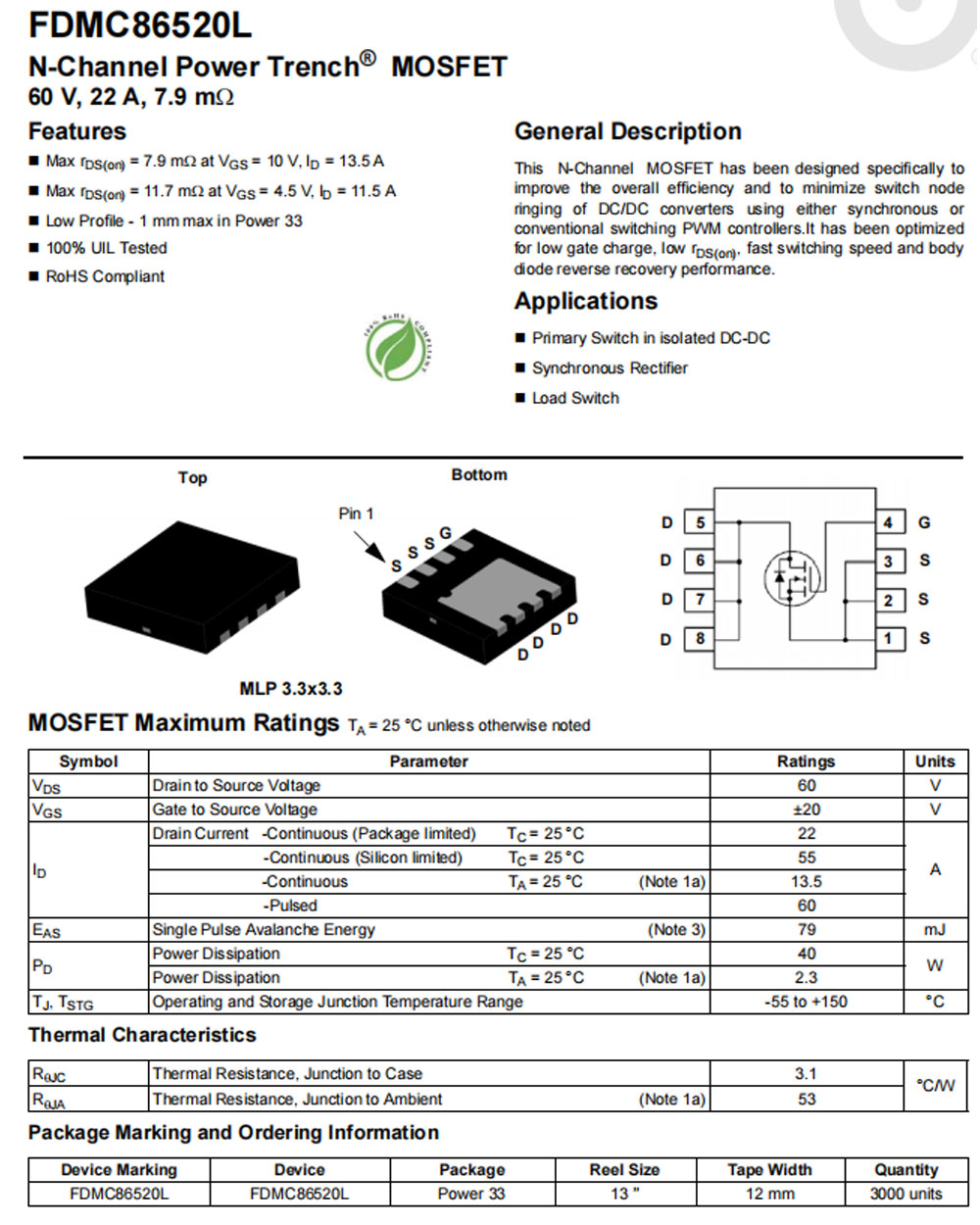
FDMC86520L
Produktbeskrivelse
Features Of FDMC86520L
Max rDS(on) = 7.9 mΩ at VGS = 10 V, ID = 13.5 A
Max rDS(on) = 11.7 mΩ at VGS = 4.5 V, ID = 11.5 A
Low Profile - 1 mm max in Power 33
100% UIL Tested
RoHS Compliant
General Description of FDMC86520L
This N-Channel MOSFET has been designed specifically to improve the overall efficiency and to minimize switch node ringing of DC/DC converters using either synchronous or conventional switching PWM controllers. lt has been optimized for low gate charge, low rDS(on, fast switching speed and body diode reverse recovery performance.
Applications of FDMC86520L
Primary Switch in isolated DC-DC
Synchronous Rectifier
Load Switch
MOSFET Maximum Ratings of FDMC86520L
TA=25℃ unless otherwise noted
Thermal Characteristics
Electrical Characteristics of FDMC86520L
TJ=25℃ unless otherwise noted
Off Characteristics
On Characteristics
Dynamic Characteristics
Switching Characteristics
Drain-Source Diode Characteristics
NOTES:
1. RθJA is determined with the device mounted on a 1 in2 pad 2 oz copper pad on a 1.5 x 1.5 in. board of FR-4 material RθJC is guaranteed by design while RθCA is determined by the user's board design.
2. PulseTest: Pulse Width